Chips Are Now Fused Together With No Solder at All
By aligning copper pads and heating them, makers get shorter, denser links between stacked chips.
 Dwarkesh Podcast · What will computer chips look like in 2045?
The newest way to join computer chips uses no solder at all. Copper meets copper, insulation meets insulation, and heat fuses them into one electrical whole.
The job is packaging, the step after a chip is made when it must be linked to neighboring chips and the rest of the computer.
To pack in more connections, the industry added a shared silicon platform known as an interposer that holds several chips.
Chips then talked through wiring that runs directly through that platform, an approach known in the industry as 2.5D.
A different method stacks one chip atop another for shorter links. Early versions used solder bumps, but those bumps are bulky and increase electrical resistance.
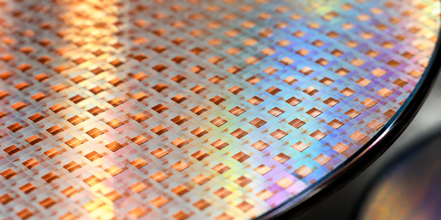
Hybrid bonding skips the solder. Makers line up the copper signal contacts on the first chip with matching contacts on the second, press the chips together, and heat them.
The heat makes the copper expand and bridge the tiny gap between the chips. At the same time, the non-conductive layers surrounding the copper also join, leaving much denser connections.
It took years to make that simple idea work in factories. Alignment and defect problems needed years of work to solve, which delayed volume manufacturing.
There are two ways to do it, said Tyler Osborne, who leads work in Intel's advanced packaging team. In wafer to wafer bonding, two full wafers are joined at once.
That method works when the two designs match, and it dominates in camera image sensors. The catch is yield: if a good spot on one wafer happens to meet a bad spot on the other, a good chip is wasted.
In die to wafer bonding, makers cut up one wafer, test the small chips, and then attach only the known good ones to good sites on the other wafer. Intel expects to use both methods, depending on the customer and the design.
The payoff is steady shrinkage. In the October 2026 interview, Osborne said the spacing between connections, called pitch, was 130 to 150 micrometers about 15 years ago. By the time of the interview, it was 25 micrometers in high volume production, and sub 10 micrometers in the lab.
Questions people ask
What does pitch mean in chip packaging?
Pitch is the center to center distance between neighboring electrical connections. A smaller pitch means more connections can fit in the same area, so chips can exchange more data at once.
Why is skipping solder better for performance?
Shorter, direct copper joints have less electrical resistance than bulky solder bumps, so they waste less energy as heat. They also allow signals to travel a shorter distance, which saves time and power.
Does this replace making transistors smaller?
They address different problems, and the source does not claim one replaces the other. Shrinking transistors packs more computing into one chip, while hybrid bonding packs more communication between chips. For AI workloads that move huge amounts of data, the links between chips can matter as much as the transistors themselves.